ELECTRONICS PRODUCTION
GOALS FOR THE WEEK
- Characterize the design rules for your in-house PCB production process: document feeds, speeds, plunge rate, depth of cut (traces and outline) and tooling.
- Document your work to the group work page and reflect on your individual page what you learned
- Make an in-circuit programmer that includes a microcontroller by milling and stuffing the PCB, test it to verify that it works.
GROUP
INDIVIDUAL
MILLING MACHINE AND BITS
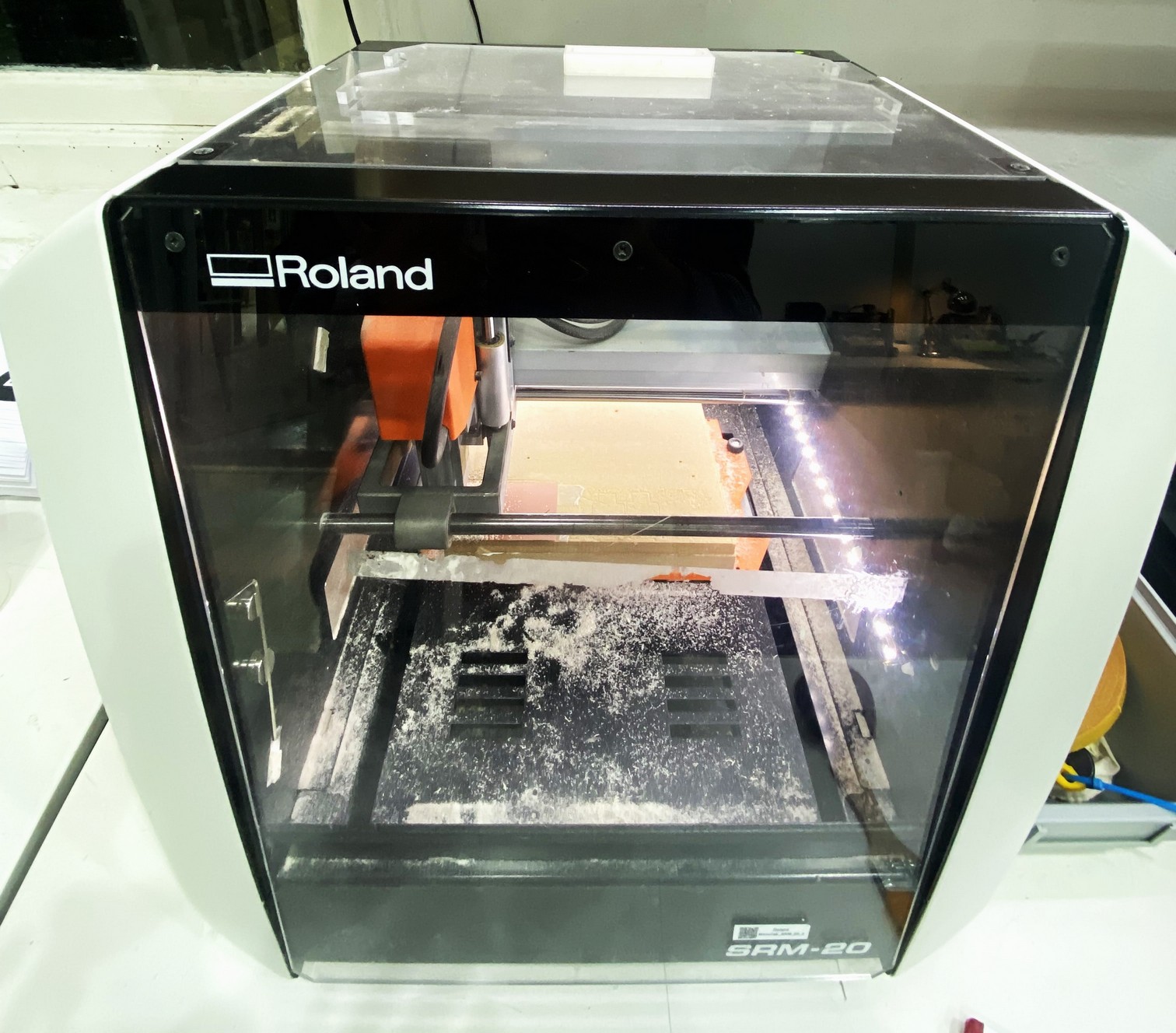
SRM 20
The SRM-20 is capable of cutting a wide variety of materials, including chemical wood, acrylic, and ABS. It is also capable of a range of accuracy settings from prototype to product design. It has a VPanel controller to regulate feed rate, spindle speed and milling on X, Y, Z axes, and an independent system that allows for setting of the Z-axis point and tool changes.
GROUP ASSIGNMENT
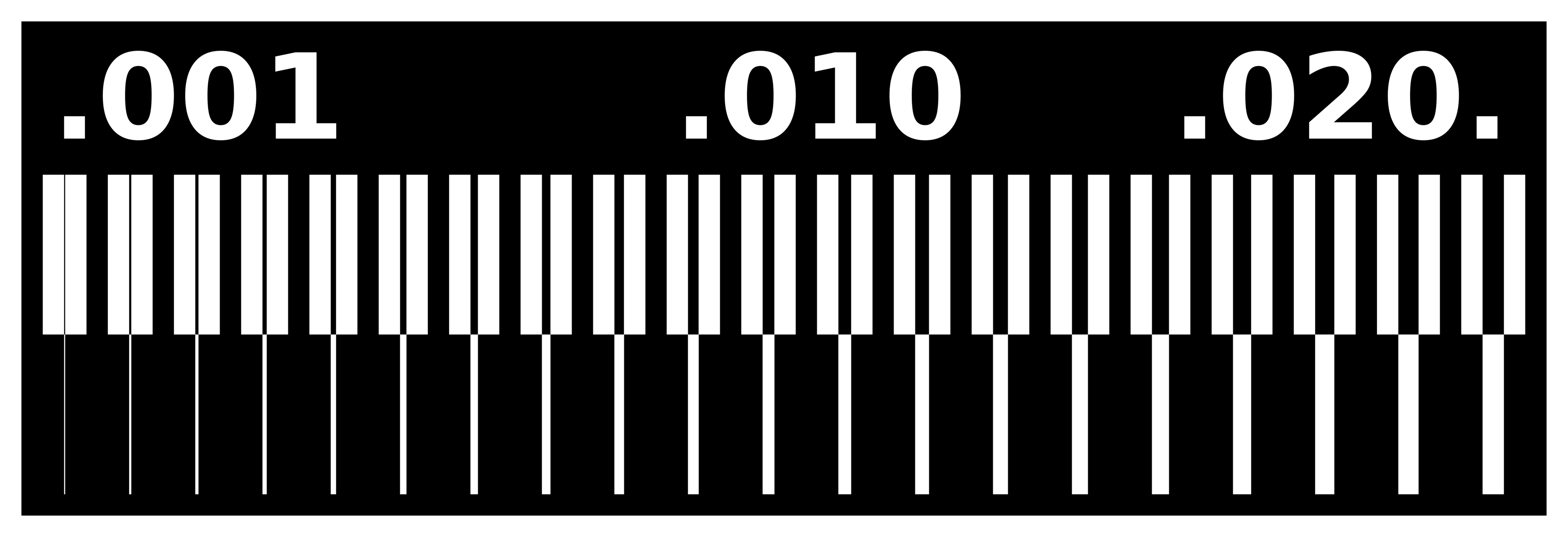
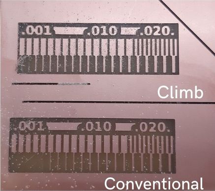
For the group assignment, we decided to work in pairs and each take up a test with different parameters in order compare the results.
Me and Ximena decided to mill the line test in conventional mode, while another team tested in Climb mode
The group page is linked here
THE TEST
SETTING UP THE FILE
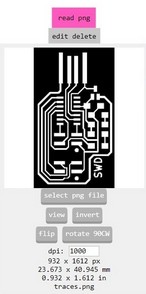
I used Modsproject.org to set it up.
FOR TRACES
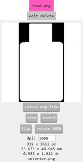
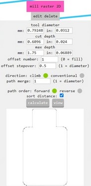
- I uploaded the Png file into Readpng. I kept the dpi size 1000 as changing it would change the size of my file.
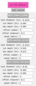
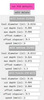
- Set the PCB Defaults to mill trace 1/64 and changed the speed to 3.
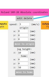
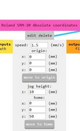
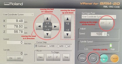
- I set the Roland SRM-20 Absolute coordinates with speed as 3, xyz orgins to 0, the jog height as 10 and home with Z as 50mm.
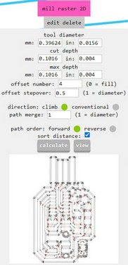
- In Mill raster 2D, the offset number has to be 4 and the direction 'climb', after which I clicked on Calculate which downloaded the rml file.
FOR OUTLINE CUTS
- Set the PCB Defaults in mill traces 1/32 and change the speed to 1.5.
- I set the Roland SRM-20 Absolute coordinates with speed as 3, xyz orgins to 0, the jog height as 10 and home with Z as 50mm.
- In Mill raster 2D, the offset number has to be 4 and the direction 'climb', after which I clicked on Calculate which downloaded the rml file.
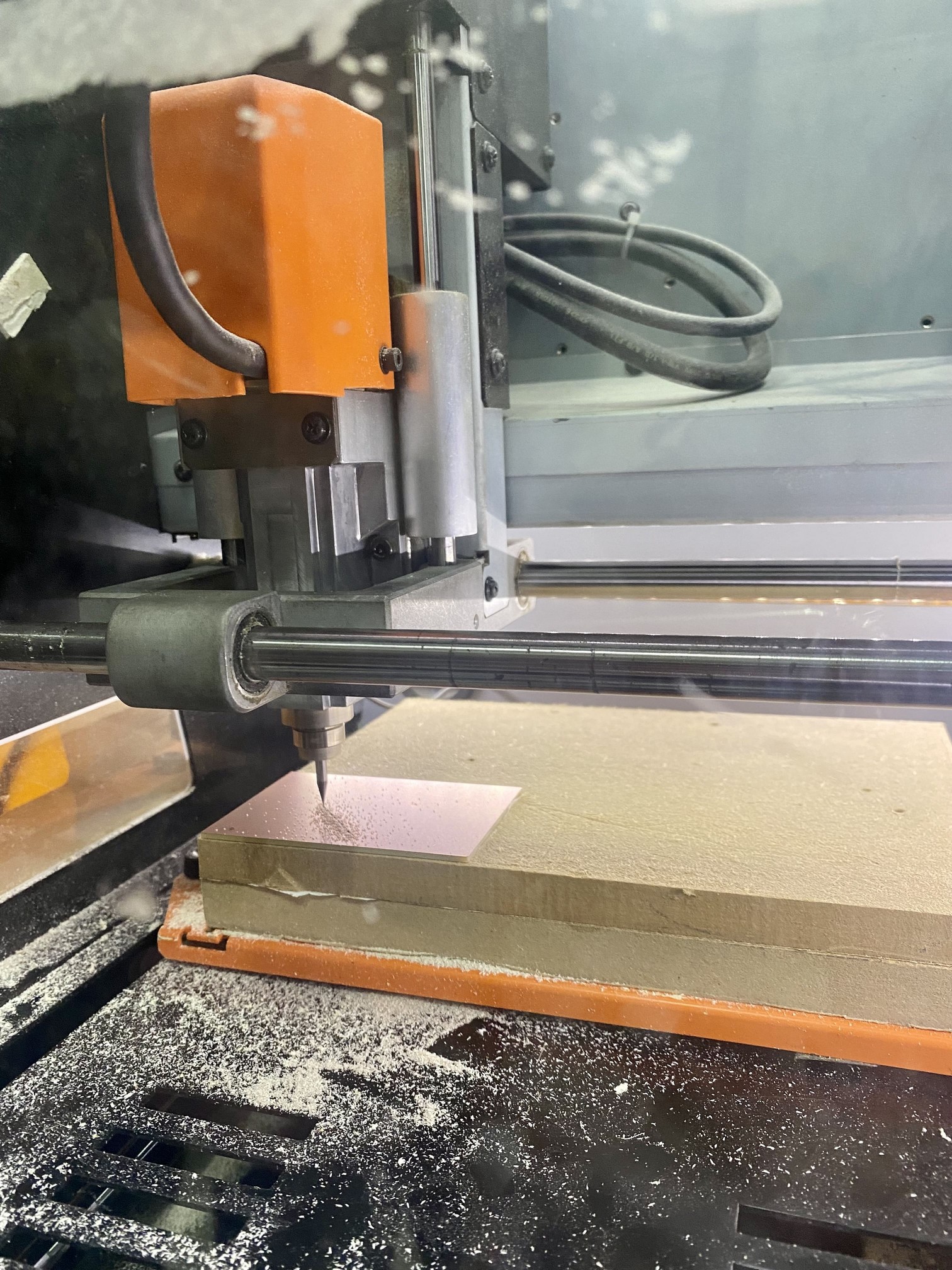
setting up the machine
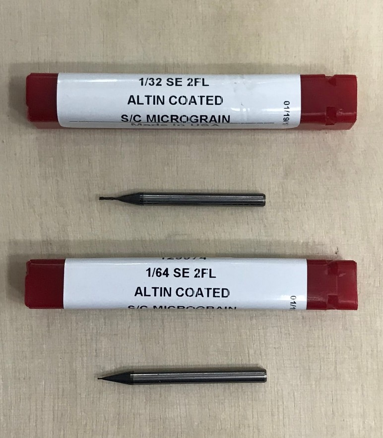
- First, for the traces, I set the 1/64 milling bit in place and tightened it with an Allen key.
- Stick board to the Bed with double-sided tape and set the XY origins by moving the head to where I wanted the milling to start.
- Set the Z origin by moving the bit to the point where it touches the board.
- 'Cut' option lets you upload the rml file and 'output' starts the milling.
COMPARING THE RESULTS
INDIVIDUAL PROJECT
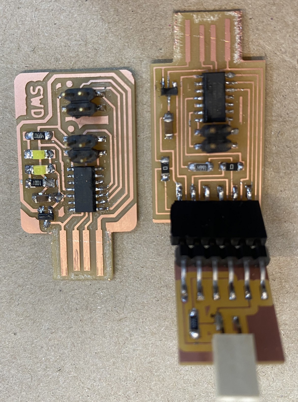
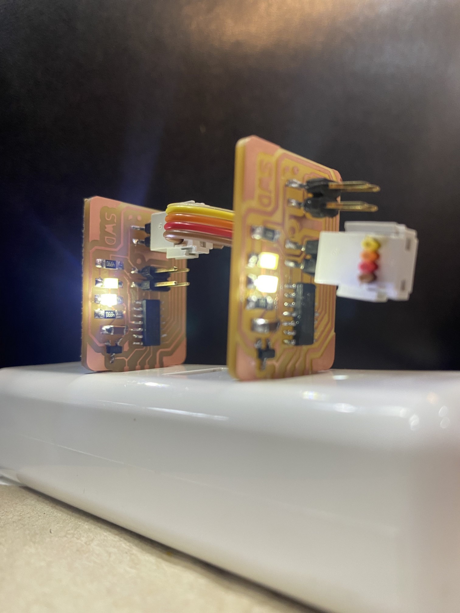
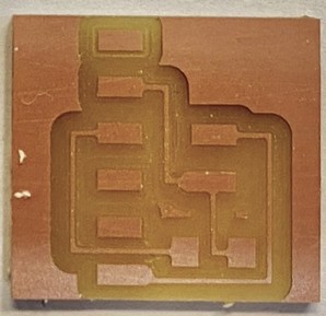
After testing out the machines, we had to mill our own PCB Boards. Decided to mill and stuff 3 different boards.
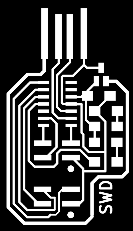
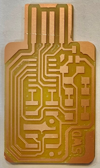
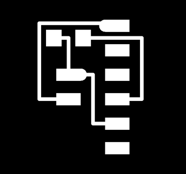
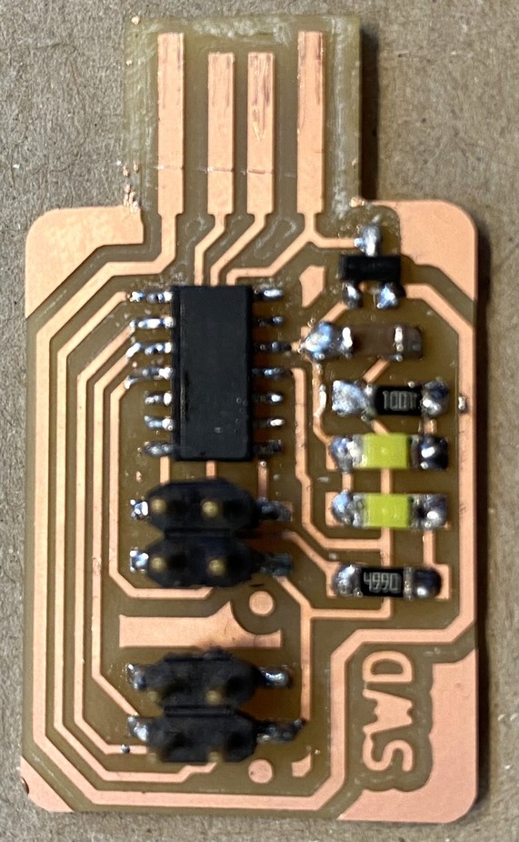
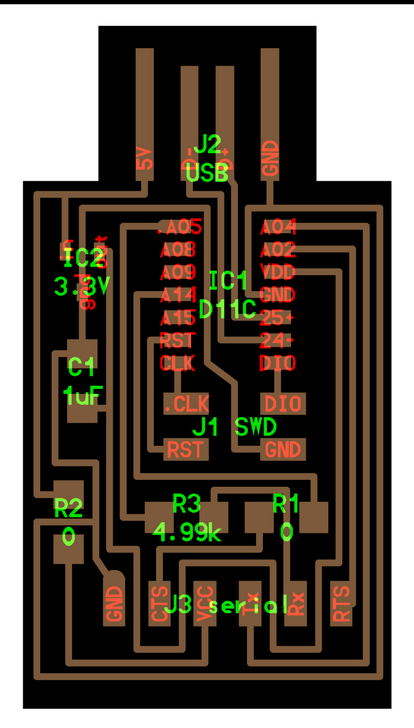
- SWD D11C
D11C-based programmer with SWD connector for programming ARM chips such as D11C itself - Serial D11C
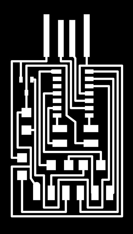
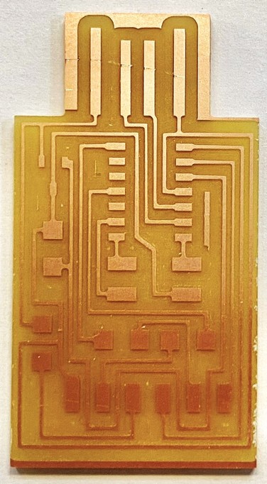
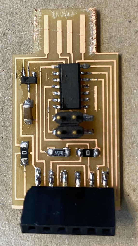
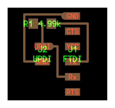
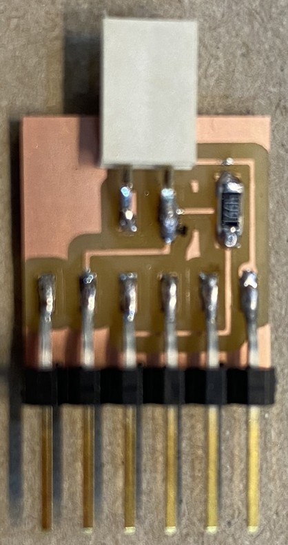
D11C-based USB to serial bridge for debugging and programming using serial port. - Serial to UPDI
Adapter to convert one of the serial (FTDI) bridges into an UPDI programmer.
SWD D11C
- Minimal BOM.
- Foolproof connectors with a mark on GND pin.
- LED's
Serial D11C
- Minimal BOM.
- 5V-tolerant serial, 5V power to target.
Serial To UPDI Adapter
SWD D11C
Serial D11C
Serial To UPDI Adapter
- I had to made a seperate folder consisting of the binary code and edbg application exe.
- Connect the SWD to your laptop.
- Open the folder in Gitbash and run edbg -ebpv -t samd11 -f free_dap_d11c_mini.bin
The Design files can be found here
D11C-based programmer with SWD connector.
The main features are:
To get the .rml file for milling, I used modsproject.org. The settings used are the same as the Group project.
The specifications and
workflow for which are under the Group Project
THE BOARD

Rml files download
Traces
Outline
DD11C-based programmer/debugger with a serial FTDI socket.
The main features are:
To get the .rml file for milling, I used modsproject.org. The settings used are the same as the Group project.
The specifications and
workflow for which are under the Group Project.
THE BOARD

Rml files download
Traces
Outline
A basic adapter board to turn your serial (FTDI) programmer/debugger into an UPDI programmer.
To get the .rml file for milling, I used modsproject.org. The settings used are the same as the Group project.
The specifications and
workflow for which are under the Group Project.
THE BOARD

Rml files download
Traces
Outline
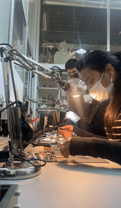
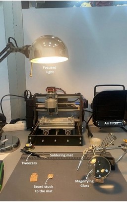
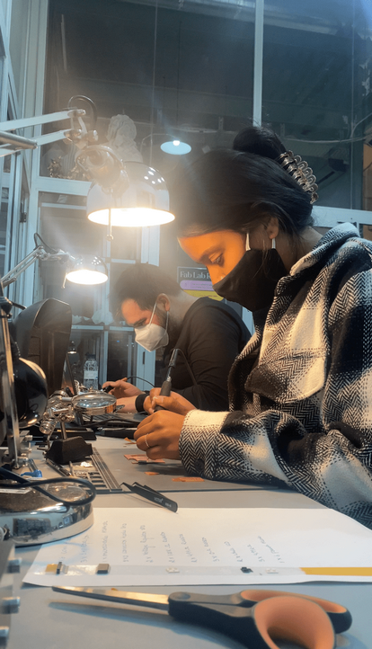
SOLDERING
After milling the PCB's, I had to solder all the componenets to it.
Soldering is a welding process creating a joint between two conductive
leads or metal surface by hearting and tinning ,mostly iron and copper.
The SETUP,
The key is to take your time, use good lighting and some copper wire to cover up your mess.
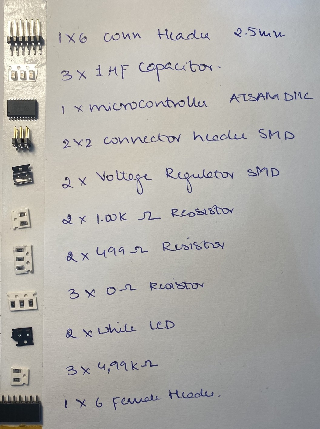
Link to Components list interactive BOM
PROGRAMMING THE SWD BOARD
The board had to be flashed with the free dap binary from Alex Taradov, which can be downloaded here
For flashing, edbg can be used with the following command: edbg -ebpv -t samd11 -f free_dap_d11c_mini.binAs a windows user,
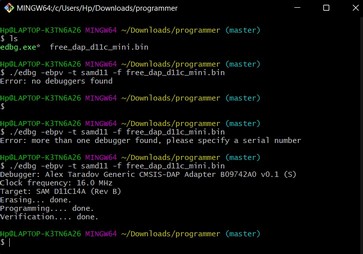
And the Board is Programmed!